


Odisha to Fast-Track 1,000-Acre Semiconductor Cluster Near Bhubaneswar
State targets global investments, promises lowest power tariffs and faster clearances to boost electronics hub

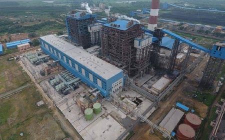
Bhubaneswar: The Odisha government has unveiled plans to establish a 1,000-acre Semiconductor and Electronics Manufacturing Cluster near Bhubaneswar airport, aiming to position the state as a frontrunner in India’s growing semiconductor industry.
The project will host key facilities, including the SiCSem and 3D Glass units, both recently approved by the Centre and state government. Officials confirmed that land has been identified and groundwork is underway, with construction expected to begin soon. The foundation stone for the SiCSem project will be laid next month.
State IT Minister Dr. Mukesh Mahaling said the government is working with Malaysian engineers to bring in global expertise. “While such plants usually take two years, our goal is to make them operational within 18 months,” he stated.
To ensure smooth operations, Odisha is engaging industrial gas suppliers, chemical manufacturers, and raw material providers. Land has also been reserved for ancillary industries to strengthen the supply chain.
The government is offering concessional power tariffs—claimed to be the lowest in India—along with a new Semiconductor Policy targeting 120 chip design companies by 2030.
Odisha showcased its semiconductor ambitions at *Semicon India 2025* in New Delhi, where MoUs worth ₹2,655 crore were signed, including ₹1,650 crore by Sancode Technologies and ₹1,005 crore by Top Track Hitech PCB Pvt Ltd. Last month, the Union Cabinet also cleared two semiconductor projects worth ₹4,009 crore in the state.
Chief Minister Mohan Charan Majhi said the initiative aligns with the vision of transforming Odisha into a hub for advanced electronics, creating jobs, innovation, and global investment opportunities.
What's Your Reaction?