


Semiconductor Era Begins in Odisha with Mega Investments
From Jajpur to Bhubaneswar, chip manufacturing projects mark a new industrial era for Odisha
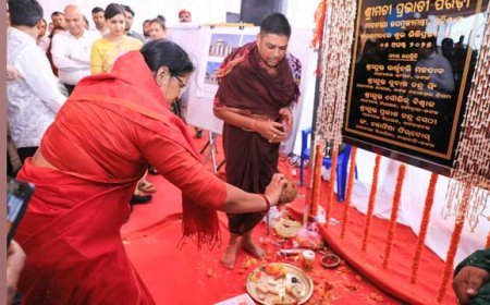
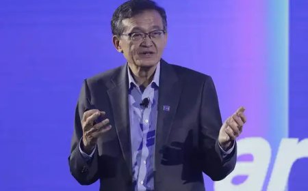
Bhubaneswar: Odisha is set to script a historic chapter in India’s semiconductor journey, with Intel CEO Lip-Bu Tan expected to visit the state later this year for the groundbreaking of 3D Glass Solutions’ (3DGS) packaging unit at Jajpur’s Kalinga Nagar.
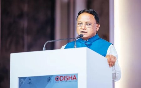
Principal Secretary of Electronics and IT, Vishal Kumar Dev, said the groundbreaking of SicSem’s Silicon Carbide (SiC) fabrication unit will take place next month, while 3DGS awaits Tan’s visit for its launch.
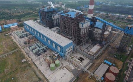
The 3DGS unit, backed by Intel, Lockheed Martin, and Applied Materials, involves an investment of ₹1,943 crore and targets annual production of 5 crore units. The project is expected to generate 1,500 direct and nearly 5,000 indirect jobs.
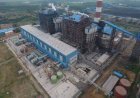
Separately, SicSem, in collaboration with UK-based Clas-SiC Wafer Fab, will establish India’s first SiC-based compound semiconductor fabrication facility in Bhubaneswar. Another player, RIR Power Electronics, has invested ₹618 crore, with commercial production planned for 2026.
Odisha’s revised semiconductor policy, offering incentives and stipends to engineering students, is aimed at attracting talent and investments. Together, these projects position the state as a rising hub in India’s semiconductor ecosystem.
What's Your Reaction?